Fine-line screen printing with low-temperature pastes
The requirements with respect to realising finer structures and tracks continue to increase. Major demands are made not only of the application process and the screens used but also of the development of the pastes.
Many factors play a crucial role in this development, such as the final line width, the gap between structures, the overall layer structure or the substrate. The result is that there is no universally usable product and attention must be paid to the specific requirements even when developing the pastes.
The following examples are intended to highlight how different such requirements can be.
1.Solar technology: single-layer fine-line printing
The solar sector will play a growing role in our future. Developments are steadily progressing, bringing with them new challenges for the materials and production processes used.
One technology on which development work is currently focusing is the so-called tandem solar cell. In this process, two solar cells are combined to use a broader range of the sunlight spectrum and ultimately to increase efficiency. Perovskite materials are used here which are sensitive to both moisture and temperature.
This in turn means that the standard high-temperature production processes can no longer be used.
From the perspective of paste development, the particular challenges here lie in the printing of very fine finger structures with the highest possible aspect ratio and smooth topography. It must be possible to process these pastes in the shortest amount of time at temperatures < 150°C and they must compete with the products currently used with respect to electrical conductivity.
2. Safety concepts: multilayer fine-line printing
In the case of multilayer structures, the challenges can be completely different although no less complex. Here the task is to apply many fine tracks in a small space keeping the gaps as low as possible in order to build several layers in the second stage of the process.
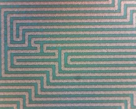
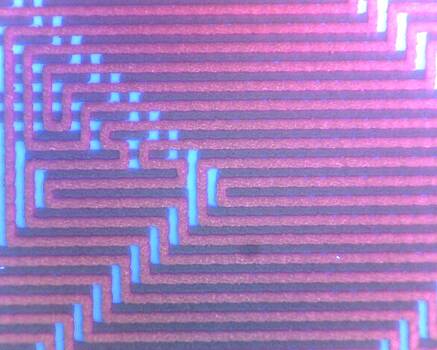
In this case, special challenges are posed not only to the development of the electrically conductive material, but also to the insulating layer in between. The role of this layer is to completely cover the printed tracks and offer a base, ideally comparable with the substrate, for printing further tracks on top. Factors such as surface energy and smoothness play an important role here to facilitate the precise printing of tracks without decreasing the flowing behavior.
At ELANTAS Europe, development focuses on offering a set of electrically conductive and insulating products that is tailored to the application.
Conclusion: Fine-line printing is a very broad term that can make different demands on the materials deployed depending on the application. It is therefore important from the perspective of the paste development to understand the demands made on the final application at an early stage to enable the precise needs to be addressed and the right materials to be selected.
Another challenge is the precise production of printed functionalities in scalable processes. Witte Technology is a pioneer in the field of multi-layer conductor track production under series conditions. At Witte Technology GmbH, experts are available to answer questions about printed electronics and to organise series production in collaboration with ELANTAS Europe.
We will be happy to answer any queries you may have directly and to support you in the technical implementation of your projects with the appropriate products. Simply send us an email to: AdvancedPrinting@altana.com
You can find more detailed information on the products mentioned on the links below. You can find appropriate recommendations for further insulating and conducting screen-printing pastes there and in our technical data sheets.